Advanced Applications
Advanced Semiconductor & Electronics Forming Solutions
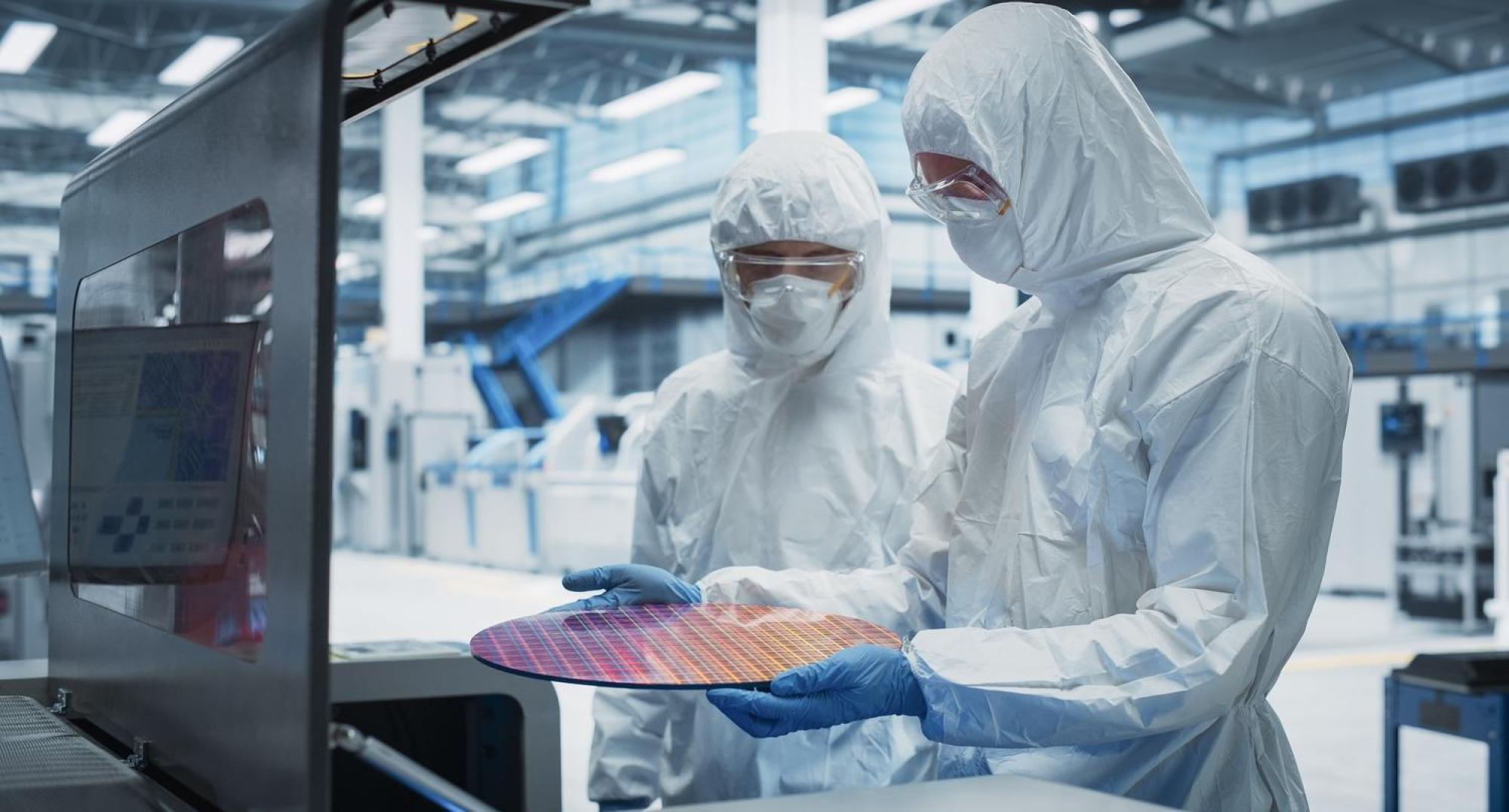
Co-Developing High-Precision Forming Systems for Wafer and PCB Manufacturing
In advanced semiconductor and electronics manufacturing, equipment is more than a tool—it is an integral part of the process.
At Tung Yu, we work closely with customers to co-develop forming, bonding, and lamination solutions that meet the demanding requirements of wafer, PCB, and advanced electronics production.
Moving beyond standard machinery, we prioritize deep process collaboration — engineering systems together with your team to address thermal, pressure, and material challenges in real manufacturing environments.
Our Process-Driven Approach
We Start with Your Process, Not with a Machine
Every semiconductor or electronics project involves unique materials, layer structures, and quality requirements. At Tung Yu, we begin by understanding your process flow, potential defect risks, and yield targets, and then design forming systems tailored to those requirements.
Co-Engineering with Your Technical Team
We work side by side with your process engineers to:
- Define optimal pressure, temperature, and vacuum profiles
-
Optimize bonding and lamination sequences
-
Protect fragile wafers and substrates from warpage and mechanical stress
From Lab Trials to Pilot Lines and Scale-Up
Whether you are validating a new wafer structure, testing a new PCB stack-up, or scaling a new electronics product, we support you through:
-
Process trials
-
Pilot equipment design
-
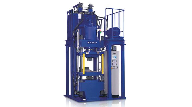
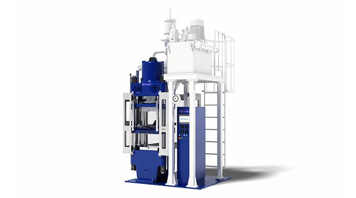
Production-Ready All-Electric Servo Presses and Hydraulic Forming Solutions
Core Process Solutions
Our forming and bonding systems are engineered to handle a wide range of advanced materials used
in semiconductor and electronics manufacturing, including:
-
Wafer Bonding & Thin Film Technologies
-
High-Speed Signal & PCB Foundation Materials
-
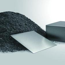
High-Performance Electronic Ceramics
-
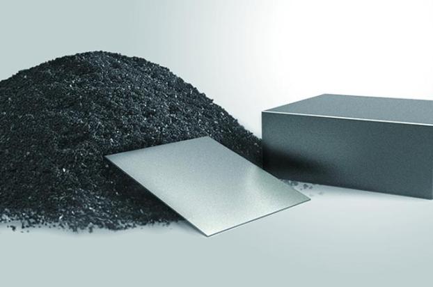
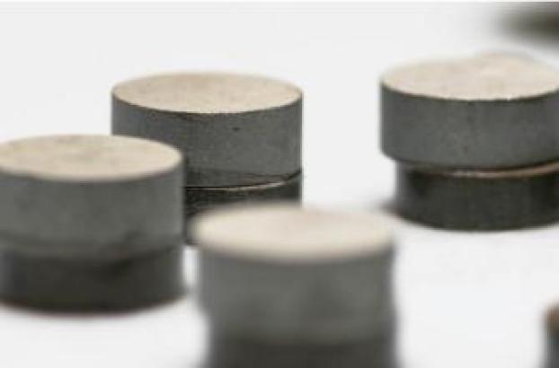
Advanced Functional Powder Metallurgy
Focus Areas in Semiconductor, Wafer & PCB Applications
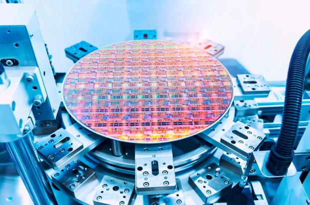
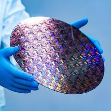
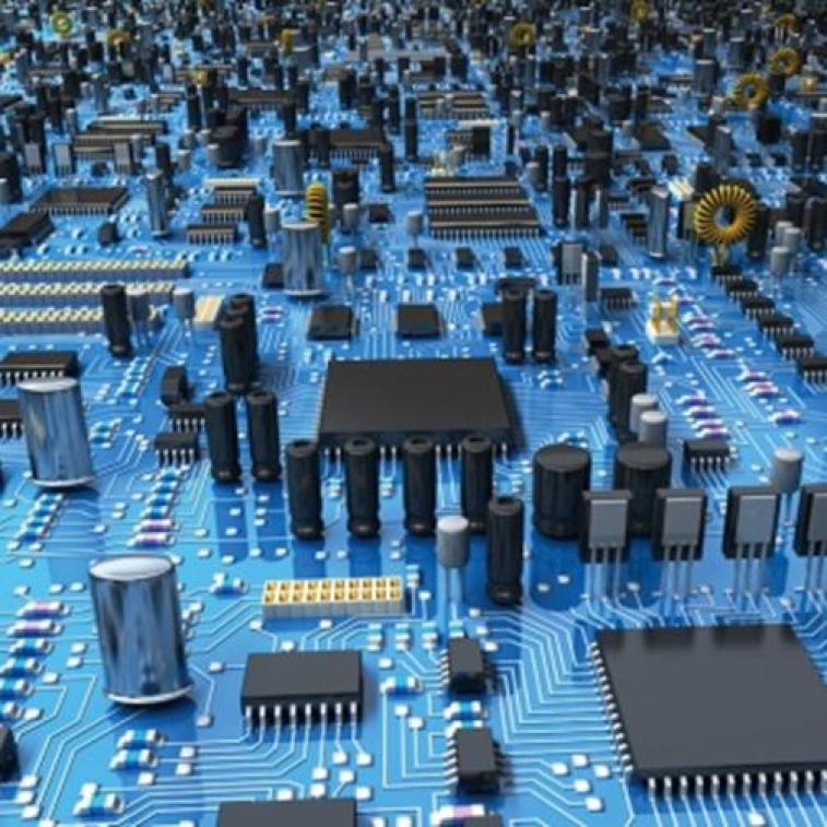
Wafer Bonding & Advanced Packaging
Every semiconductor or electronics project has unique materials, layer structures, and quality requirements. At Tung Yu, we begin by understanding your process flow, potential defect risks, and yield targets, and then design forming and bonding systems tailored to those requirements.
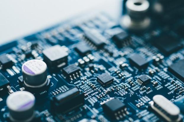
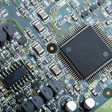
High-Density PCB & Substrate Lamination
For HDI and multilayer PCB production, we support precision lamination processes focused on:
-
Accurate layer alignment
-
Thickness uniformity
-
Thermal stress reduction
Electronics Vacuum Molding & Composite Substrates
We work with advanced insulation materials and composite substrates used in high-performance electronics.
Together with customers, we develop optimized molding and curing profiles to ensure stable product quality and manufacturing reliability.
What We Help You Build
Advanced components and structures co-developed for next-generation semiconductor and electronics manufacturing.
Semiconductor & IC Substrates

Consumer Electronics

Smart Wearable Technology
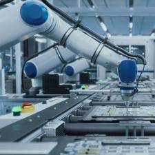
Robotics & Industrial Automation

IoT & Smart Connectivity
Power Electronics & Energy
High-Frequency Communication
Advanced Material Processing

What You Can Expect from Working with Tung Yu
-
A process-first mindset, not a catalog-driven approach
-
Engineering teams willing to engage in your manufacturing challenges
-
Flexible machine design based on your materials and targets
-
Long-term collaboration from development to production
Let’s Build Your Process Together
If you are developing next-generation semiconductor devices, advanced PCBs, or high-reliability electronics, Tung Yu is ready to co-create the forming and bonding systems your process requires.
__25L08e8ZxA.jpg)
__25L01nXeiP.jpg)
__25L089js2S.jpg)
__25K10JOEh7.jpg)